Руководство по ремонту хэш-платы Antminer T17 [EN]
Editor-in-Chief: Li Yan
Version date: 2019.7.2
File Category: Maintenance Plan
Content of this Volume: It mainly describes the troubleshooting of various faults of T17, and how to use the test
tool for accurate positioning.
I. Maintenance Tools
1. General electric screwdriver
2. Fluke 15b+ Multimeter, tweezers, V9-v1.2 test jig, T17 chassis with power set
3. Hot air gun (welding temperature is 260 degrees±2 degrees)
4. Constant temperature soldering iron (welding temperature is 300-350 degrees)
5. Environmentally friendly flux solder paste, lead-free low temperature (melting point at 150 degrees) solder wire, anhydrous alcohol, water for cleaning panel,
6. OM550 low temperature solder paste, BM1397AE tinning steel mesh jig
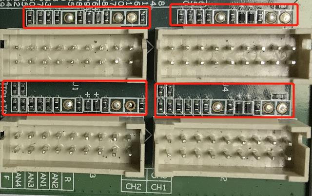
II. Component Structure of the Hash Board

III. Signal Transmission Circuit
1. Signal transmission channel, signal CLK-RST-BO-CO is transmitted from the first chip to the second, and till the 72nd, RI signal is reversely transmitted from the 72ndchips to the first chip, as the figure below:

2. Signal test point identification and test point arrangement order (there are a total of 48 chips on the hash board, and 12 voltage domains), as shown below:

Distribution of test points in voltage domain


3. Signal communication circuit from IO socket to chip

Picture of J1-IO socket
 Schematic diagram of J1-IO socket


IV. Power Circuit
1. The power supply voltage of each board is (T17 jig test voltage output is 17V). There are 10 voltage domains, and the voltage of each two voltage domains is 1.7V.

V. Cases of Single Board Test Troubleshooting
5.1 Single board jig test asic=0
Failure analysis:
1. Whether the jig cable and hash board are in good contact.
2. The T17 hash board J6-J7 should have a voltage of 17V when testing the jig.
3. When testing the jig, measure whether there is voltage between the 10 voltage domains.
3.1 If there is no voltage in the voltage domain, it is necessary to see whether the normal working voltage of the pin 4 of Q7, Q8, Q9, Q11 is low level of 0V. If it is high level, then it depends on whether the pin 1 of Q10 is high level of 3.3v, if Q10 does not have 3.3V Voltage, that is, U3-PIC loses firmware or there is no power supply.

Schematic diagram of PIC

17V output control circuit

3.2. If the power supply is normal and there is voltage in voltage domain, then the RI signal of the chip should be measured to see if the RI signal has a voltage of 1.8V. When measuring the RI signal, it should start from the test point of the last chip. If there is voltage in the last chip, measure whether the 20th chip has RI -1.8v, and the rest can be done in the same manner, when finding the chip that does not have RI output voltage, first measure the 1.8V power supply of this chip, if there is no power supply of 1.8V, then check the 1.8V power supply circuit. The 1.8V power supply circuit is supply powers to the LDO pin 1 through the voltage division of the voltage domain. The pin 5 of LDO outputs voltage of 1.8V. (Each voltage domain has -1.8 V LDO to supply power to chip). If there is no output, this LDO should have a problem. If 1.8V is normal, measure the ground resistance of the test point after the power is cut off and compare with the OK board to see if there is any resistance abnormality; if the resistance value is normal, and there is no problem with soldering. This chip should have a problem. (Re-tin the removed chip and solder it to a good board to verify it. If there is no RI signal, it proves that the chip is damaged, replace the chip.)
1.8V power supply circuit


5.2 Fault phenomenon is ASIC=7
Analysis: ASIC=7,
1. In a single board test, 7 chips can be found. It can be judged that the RI signal is normal. If the 8th chip cannot be found, we will directly measure the voltage of the 7th chip U198-CLK-RST-CO to see if the power supply is normal. If CLK does not have a voltage of 0.8V, then it depends on the power supply circuit of CLK.
2-CLK circuit analysis: If CLK does not have 0.8V, first check whether the 0.8V power supply of the bad chip voltage domain is normal, the 0.8V power supply circuit is obtained by voltage domain division, and 1.8V power supply mode is the same, as for the maintenance method for pin 5 output 0.8V, refer to the 1.8V maintenance method (note that there are 2 out of 3 chips outputting 0.8V LDO power supply in each chip in each domain of T17, and each LDO supplies to 2 chips).
0.8v power supply schematic


If the 0.8V power supply circuit does not have a 0.8V output, then see if the 0.8V LDO power supply has a supply voltage of about 3.2V. If it has, see if the LDO is soldered insufficiently or short-circuited. If there is a 0.8V output, then see the ground resistance of the chip, if the resistance is correct, it should be a bad chip.
По вопросам приобретения продукции обращайтесь к нашему менеджеру по продажам:![]() [email protected]
[email protected]
По вопросам ремонта майнера и послепродажного обслуживания обращайтесь к менеджеру по ремонту:![]() [email protected]
[email protected]
По вопросам делового сотрудничества обращайтесь:![]() [email protected]
[email protected]
ЖАЛОБЫ И ПРЕДЛОЖЕНИЯ
Если вы недовольны транзакцией или у вас есть ценные предложения для нас, свяжитесь с нами по этому адресу электронной почты:![]() [email protected]
[email protected]
Скачать и просмотреть руководство по ремонту, запуску и обслуживанию асик майнеров AntMiner, Whatsminer, Innosilicon, Avalon онлайн
На этой странице вы можете прочесть и скачать все необходимые руководства.
Но, конечно, вы всегда можете связаться с нами по WhatsApp +79275104327, по электронной почте Этот адрес электронной почты защищен от спам-ботов. У вас должен быть включен JavaScript для просмотра. или оставить сообщение в чате, если у вас есть какие-либо (технические) вопросы о наших продуктах.
Руководство по ремонту [PDF] Antminer
Руководство по ремонту хэш-платы Antminer D3
Руководство по ремонту хэш-платы Antminer S9
Руководство по ремонту хэш-платы Antminer S9K
Руководство по ремонту хэш-платы Antminer S11
Руководство по ремонту хэш-платы Antminer S15 T15
Руководство по ремонту хэш-платы Antminer S17+
Руководство по ремонту хэш-платы Antminer S17E
Руководство по ремонту хэш-платы Antminer S17
Руководство по ремонту хэш-платы Antminer T9
Руководство по ремонту хэш-платы Antminer T17+
Руководство по ремонту хэш-платы Antminer T17
Руководство по ремонту хэш-платы Innosilicon miner
Руководство по ремонту хэш-платы Antminer WhatsMiner M10
Руководство по ремонту хэш-платы Antminer Whatsminer M20S
Инструкция по установке [PDF]
Antminer
Руководство Antminer D3
Руководство Antminer DR3
Руководство Antminer DR5
Руководство Antminer E3
Руководство Antminer L3
Руководство Antminer R4
Руководство Antminer S1
Руководство Antminer S2
Руководство Antminer S3
Руководство Antminer S4+
Руководство Antminer S5+
Руководство Antminer D3
Руководство Antminer S7
Руководство Antminer S9 Hydro
Руководство Antminer S9
Руководство Antminer S9k
Руководство Antminer S9SE
Руководство Antminer S11
Руководство Antminer S15
Руководство Antminer S17+
Руководство Antminer S17E
Руководство Antminer S17
Руководство Antminer S17Pro
Руководство Antminer T17
Руководство Antminer S19
Руководство Antminer S19Pro
Руководство Antminer T9
Руководство Antminer T15
Руководство Antminer T17+
Руководство Antminer T17E
Руководство Antminer T19
Руководство Antminer X3
Руководство Antminer Z9 Mini
Руководство Antminer Z9
Руководство Antminer Z11
Руководство Antminer Z15
Avalon
Avalonminer 1047 Manual
Avalonminer 1066 Manual
Avalonminer 1026 Manual
Avalonminer 1066 Pro Manual
Avalonminer 1146 Pro Manual
Innosilicon
Innosilicon A4+Manual
Innosilicon A6 Manual
Innosilicon A9 Manual
Innosilicon D9 DCR Manual
Innosilicon S11 Sia Manual
Innosilicon T2T 32T Manual
Innosilicon T2TZ 30T Manual
Innosilicon T3+57T Manual
Loveminer
Loveminer A1 Manual
Whatsminer
WhatsMiner D1 Manual
WhatsMiner M3 Manual
WhatsMiner M10 Manual
WhatsMiner M20S Manual
WhatsMiner M21 Manual
WhatsMiner M21S Manual
WhatsMiner M30S Manual
WhatsMiner M31S Manual
WhatsMiner M32 Manual
руководство по блоку питания и руководство по ремонту [PDF]
Руководство Antminer APW3
Руководство Antminer APW5
Руководство по ремонту блоков питания Antminer APW9 и APW9+
Руководства по Antminer, ремонт antminer , ремонт whatsminer, ремонт innosilicon, ремонт avalon, руководство по ремонту асиков
Руководство по ремонту [PDF]
Antminer
- Руководство по ремонту хэш-платы Antminer D3
- Руководство по ремонту хэш-платы Antminer S9
- Руководство по ремонту хэш-платы Antminer S9 K
- Руководство по ремонту хэш-платы Antminer S11
- Руководство по ремонту хэш-платы Antminer S15 T15
- Руководство по ремонту хэш-платы Antminer S17+
- Руководство по ремонту хэш-платы Antminer S17E
- Руководство по ремонту хэш-платы Antminer S17
- Руководство по ремонту хэш-платы Antminer T9
- Руководство по ремонту хэш-платы Antminer T17+
- Руководство по ремонту хэш-платы Antminer T17
- Руководство по ремонту хэш-платы Innosilicon miner
- Руководство по ремонту хэш-платы Antminer WhatsMiner M10
- Руководство по ремонту хэш-платы Antminer Whatsminer M20S
Инструкция по установке [PDF]
Antminer
- Руководство Antminer D3
- Руководство Antminer DR3
- Руководство Antminer DR5
- Руководство Antminer E3
- Руководство Antminer L3
- Руководство Antminer R4
- Руководство Antminer S1
- Руководство Antminer S2
- Руководство Antminer S3
- Руководство Antminer S4+
- Руководство Antminer S5+
- Руководство Antminer D3
- Руководство Antminer S7
- Руководство Antminer S9 Hydro
- Руководство Antminer S9
- Руководство Antminer S9 k
- Руководство Antminer S9 SE
- Руководство Antminer S11
- Руководство Antminer S15
- Руководство Antminer S17+
- Руководство Antminer S17 E
- Руководство Antminer S17
- Руководство Antminer S17 Pro
- Руководство Antminer T17
- Руководство Antminer S19
- Руководство Antminer S19 Pro
- Руководство Antminer T9
- Руководство Antminer T15
- Руководство Antminer T17+
- Руководство Antminer T17 E
- Руководство Antminer T19
- Руководство Antminer X3
- Руководство Antminer Z9 Mini
- Руководство Antminer Z9
- Руководство Antminer Z11
- Руководство Antminer Z15
Avalon
- Avalonminer 1047 Manual
- Avalonminer 1066 Manual
- Avalonminer 1026 Manual
- Avalonminer 1066 Pro Manual
- Avalonminer 1146 Pro Manual
Innosilicon
- Innosilicon A4+Manual
- Innosilicon A6 Manual
- Innosilicon A9 Manual
- Innosilicon D9 DCR Manual
- Innosilicon S11 Sia Manual
- Innosilicon T2T 32T Manual
- Innosilicon T2TZ 30T Manual
- Innosilicon T3+57T Manual
Loveminer
- Loveminer A1 Manual
Whatsminer
- WhatsMiner D1 Manual
- WhatsMiner M3 Manual
- WhatsMiner M10 Manual
- WhatsMiner M20S Manual
- WhatsMiner M21 Manual
- WhatsMiner M21S Manual
- WhatsMiner M30S Manual
- WhatsMiner M31S Manual
- WhatsMiner M32 Manual
руководство по блоку питания и руководство по ремонту [PDF]
- Руководство Antminer APW3
- Руководство Antminer APW5
- Руководство по ремонту блоков питания Antminer APW9 и APW9+
Mainly describe how to troubleshoot various faults of the T17e hashboard, and explains how to use the Antminer test fixture sold by ThanosMining for accurate positioning.
New version of test fixture: Antminer T17e test fixture
I. Requirements for maintenance platform / tool / equipment preparation:
1. Platform requirements:
Rubber mat maintenance platform (the platform needs to be grounded), antistatic wristband and ground connection.
2. Equipment requirements:
Constant temperature soldering iron (350–360℃), the head of tip soldering iron is used to solder small patches such as chip resistors and capacitors, etc.; heat gun, BGA rework station for chip / BGA disassembly and soldering; multimeter, soldering steel pin and shrink tubing for easy measurement (Fluke recommended); oscilloscope (Agilent recommended)
3. Testing tool requirements:
APW9 + power supply (APW9 +_14.5V-21V_V2.01 (470uF450V)) and power patch cord (selfmade) for power supply of hashboard; 2.1040 control board test fixture (fixture part number ZJ0001000001)
4. Requirements for maintenance auxiliary materials / tool:
Low-temperature solder paste Alpha OM550, flux, water for cleaning panel and anhydrous alcohol; water for cleaning panel is used to clean up soldering residues after repair; thermal conductive paste is used to apply on chips / heat sinks after maintenance (some models require thermal conductive paste); tin-planting steel mesh, ball-planting steel mesh, solder wire, solder ball (ball diameter is recommended to be 0.4mm); when replacing a new chip, you need to plant tin on chip pin and the BSM surface before soldering them to the hashboard.
5. Demand for common maintenance spare materials:0402 resistance (0R, 33R, 1K, 4.7K,); 0201 resistance (0R), 0402 capacitor (0.1uf, 1uf)
II. Maintenance Requirements:
Maintenance personnel must have certain electronic knowledge, more than one year of maintenance experience, and be proficient in BGA / QFN / LGA package soldering technology.
1. After repairing, the hashboard must be tested to be OK for more than twice, otherwise, it shall be rejected.
2. Please pay attention to the operation method when replacing the chip. There should be no obvious deformation of the PCB board after replacing any accessories. Check whether there are any open or short circuits, or missing parts in the replacement parts and the surroundings.
3. Check the tools, confirm whether the test fixtures can work normally, determine the test software parameters for the maintenance station, and version of test fixtures, etc.
4. After passing the repair and replacement chip test, you need to check the full chip before performing the functional test. The functional test shall ensure that the double-sided heat sinks are soldered OK and the cooling fan is at full speed. When using the chassis cooling function, you must put 3 hashboards at the same time to form air duct. The single-sided test of production must also ensure the formation of air ducts (important).
5. When measuring the signal, two fans are used to dissipate heat as assistance measure, and the fans maintain full speed.
6. For the front and back of the hashboard, the steel windshield is under 20V voltage. During the measurement and maintenance, please keep the maintenance table clean and insulated to avoid short circuit during the maintenance.

Figure 2-1
8. When replacing a new chip, apply solder paste on the pins and the BSM surface to ensure that the chip is pre-tinned before soldering to PCBA for maintenance.
9. Fixtures at the maintenance end adopt Repair_Mode mode and config configuration files tested in non-scanning mode. After passing the test, the production end starts the production line from test piece; the after-sale end is normally installed and aged (installed at the same level). The test configuration file can be obtained from TE.
III. Production of fixtures and precautions
The supporting clamps of the fixture should meet the requirements for heat dissipation of the hashboard and facilitate the measurement of signals.
1. Collection material number: ZJ0001000001 Test fixture.
2. Use the test fixture SD card flash program to update the control board FPGA. After decompression, copy to the SD card and insert the card into the fixture card slot. Power on for about 1 minute and wait for the control board indicator to flash for 3 times, then complete the update.

Figure 3-1

Figure 3-2
3. The test SD card will be produced according to the requirements. The single-sided heat sink uses the file before brushing to make the SD card; the double-sided heat sink uses the file after brushing to make the SD card (for batch testing of production subcontractors)
Figure 3-3
4. The double-sided test at the production end requires a code scanning gun and serial port tools. Please refer to the test process file for details.
5. The after-sale end and outsourced maintenance side does not need to use the code scanning method (fixture SD card configuration file needs to be changed, the demand can be submitted to TEand TE will test the config configuration file for fixture).
IV. Principle overview
1. T17e hashboard working structure:
The hashboard is composed of 78 BM1396 chips, which are divided into 13 groups, each group is composed of 6 ICs; the working voltage of the BM1396 chip used by the T17e hashboard is 1.35V; the last 24.5V output by the boost circuit U6 powers the LDO, LDO outputs 1.8V, the last two groups are powered by 24.5V DCDC to output 1.8V, and the other groups are powered by 17.65V divided voltage to provide 1.8V through DCDC. All 0.8V is provided by the 1.8V of this domain via the LDO output, as shown in Figure 4-1.
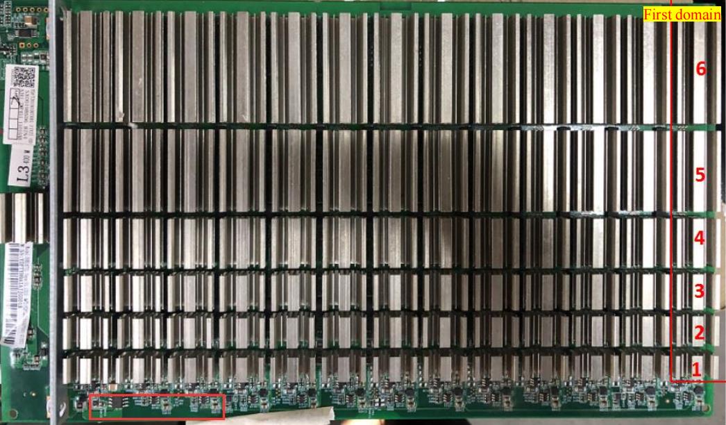
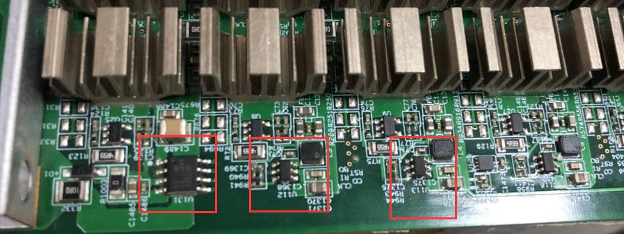
Figure 4-1
2. T17e hashboard boost circuit:
The boost is from 21V to 24.5V powered by the power supply, as shown in Figure 4-2.
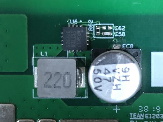
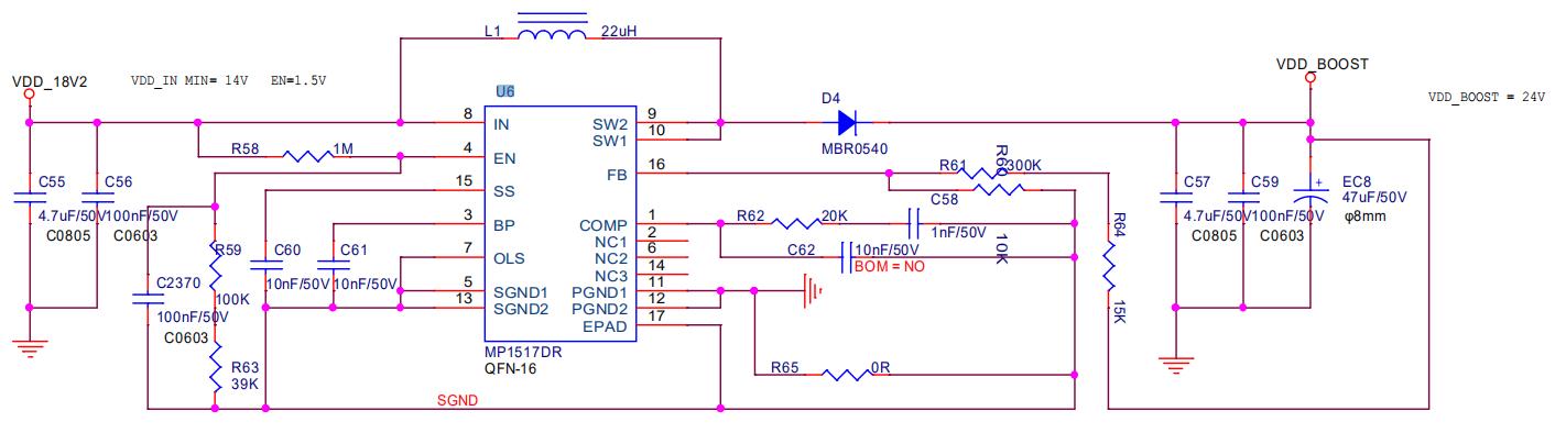
Figure 4-2
3. T17e chip signal direction:
1. CLK (XIN) signal direction: It is generated by Y1 25M crystal oscillator and transmitted from chip 01 to chip 44. During operation, the voltage is 1.45-1.65V(oscilloscope) .Multimeter measure value is about 0.7-0.9V.
2. TX (CI, CO) signal direction: input from pin 7 (3.3V) of IO port, transferred to IC U2 through level conversion, then transmitted from chip 01 to chip 78; the voltage is 0V when the IO line is not inserted, and the voltage during operation is 1.8V.
3. RX (RI, RO) signal direction: from chip 78 to chip 01, return to pin 8 of the signal cable terminal via U1 and return to the control board; the voltage is 0.3V when the IO line is not inserted, and the voltage during operation is 1.8V.
4. BO (BI, BO) signal direction: from chip 01 to chip 44; measure value is 0V when measuring with a multimeter.
5. RST signal direction: input from pin 3 of the IO port, and then transmitted from chip 01 to chip 78; 0V without IO signal or in standby and 1.8V in operation.
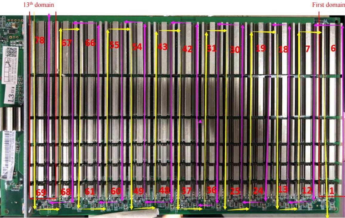
Figure 4-3
4 Overall architecture:
1. The machine is mainly composed of 3 hashboards, 1 control board, APW9 + power supply, and 4 cooling fans, as shown in Figure 3-4.
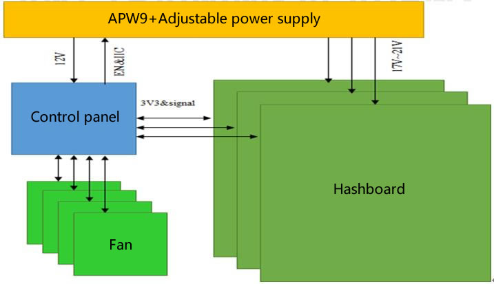
Figure 4-4
V. Common poor phenomenon of hashboard and troubleshooting procedure
Phenomenon: during single board test, chip is detected to be 0 (PT1 / PT2 station type)
Step one: check the power output first. Please check the circled part in Figure 5-1.
Figure 5-1
Step two: check the voltage domain voltage output
The voltage in each voltage domain is about 1.35V. Generally, there is a domain voltage when power is supplied at 17.65V. It is preferred to measure the output of the power supply terminal of the hashboard and determine whether the MOS is shorted (measure the resistance between pins 1, 4, and 8). If there is power supply at 17.65V but no domain voltage, continue to check downward (especially note that the voltage between each domain must be balanced, and the maximum difference cannot exceed 0.2V).
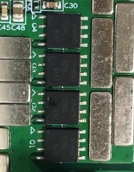
Figure 5-2
Step three: check the PIC circuit
Measure whether the second pin of U3 has an output, the voltage is about 3.2V; if yes, please continue to troubleshoot, if there is no 3.3V, please check that the connection status of the fixture cable and the hashboard is OK, and re-program the PIC.
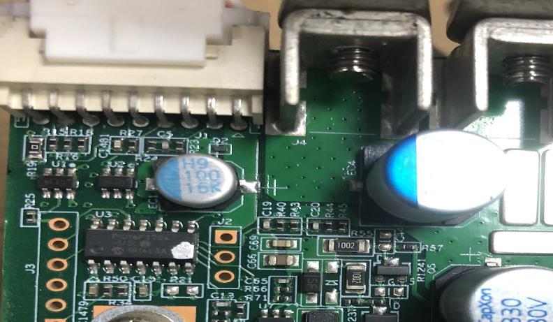
Figure 5-3
Figure 5-4
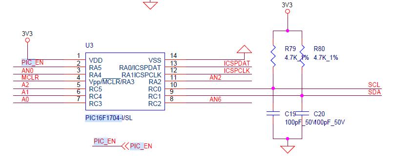
Figure 5-5
PIC programming procedure:
1. Program the PIC program of the arithmetic board.
Procedure:

Download the programming tool: PICkit3; pin 1 of the PICkit3 cable corresponds to pin 1 of J3 on the PCB, and pins 1, 2, 3, 4, 5, and 6 need to be connected.
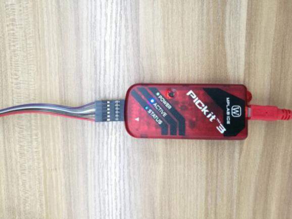
Figure 5-6
2. Programming software:
Open MPLAB IPE, select device: PIC16F1704, click power to select the power supply method, and then click operate. First step: select the file to find the .HEX file to be programmed. Second step: click connect to connect normally. Third step: click the program button, then click verify after finish. Prompt will be sent to prove that the programming is successful.
Figure 5-7

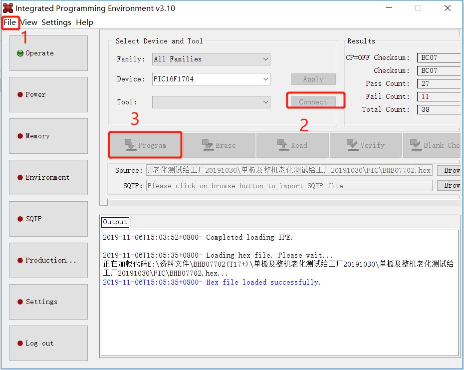
Figure 5-8
Step four: check the boost circuit output
Test D5 / D8 in chart 4-9 to measure 23-24.5V voltage.
Figure 5-9
Step five: check the LDO 1.8V or PLL 0.8V output of each group
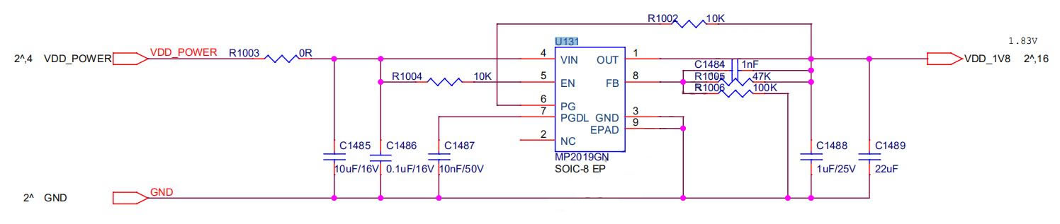
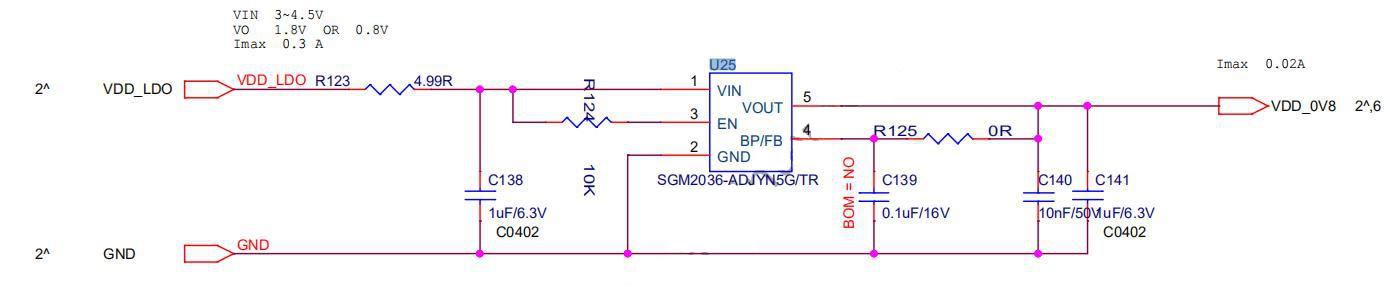
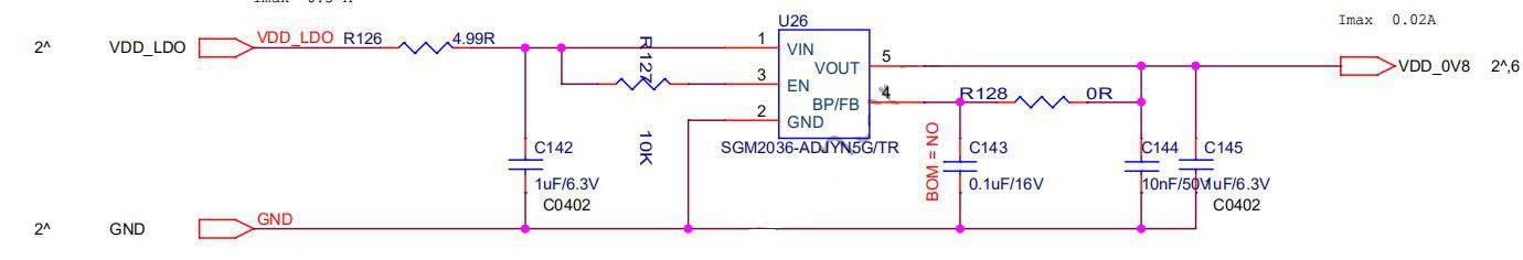
Figure 5-10
Step six: check the chip signal output (CLK / CI / RI / BO / RST)
Refer to the range of voltage values described by the signal direction. If the measurement encounters a large deviation in voltage value, it can be compared with the measured values of adjacent groups. At the same time, please note that if the input pin of the first chip of CLOK CI RSET in the first voltage domain is insufficient solder or disconnected, the single board test will return to ASIC0.

Figure 5-11
Assuming that the chip signal pin output voltage is normal, if the chip is still incomplete, for example, if 77 chips are detected, you can troubleshoot by shorting RO and 1.8V in this domain. If 77 chips can be detected after shorting, it indicate that chips 1-77 should be normal, and you can troubleshoot the 78th chip at this time. If 76 chips are detected after short-circuiting, conduct troubleshooting forward; it is recommended to adopt the dichotomy method for troubleshooting, that is, test from the middle (the 39th one is checked, and each domain can be operated in this way).
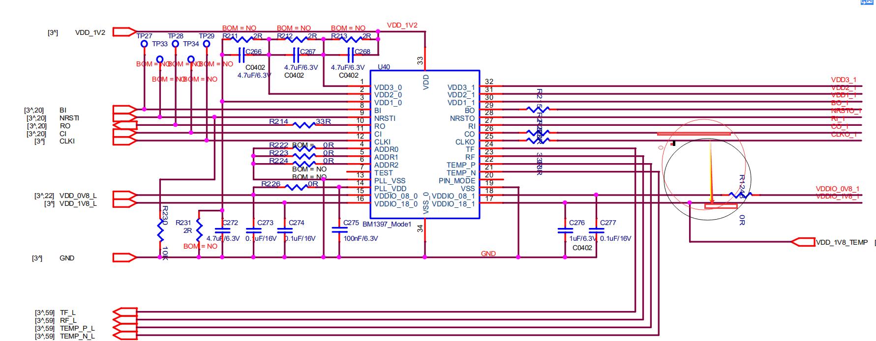
Figure 5-12
2. Phenomenon: Single board detection chip is incomplete (PT1 / PT2 station)
Check the relevant signals (CLK / CI / RI / BO / RST) of the chip in front of and behind the error position, locate the bad position according to the IC with the abnormal signal measured, and refer to the signal direction and voltage range for repair.
3. Phenomenon: single board pattern NG, that is, the response nonce data is incomplete (PT2 station type)
The serial port is connected to the computer, and the computer reads the test log; according to the results displayed in the log, the chip position of insufficient nonce data can be determined; replace the chip at the corresponding position.
4. Phenomenon: Test temperature reading is abnormal (PT2 station)
Check the temperature-sensing power supply VDD and the connection status between the temperature-sensing and the chip (TEMP_P; TEMP_N), and check the soldering quality of the chip connected to the corresponding temperature-sensing.
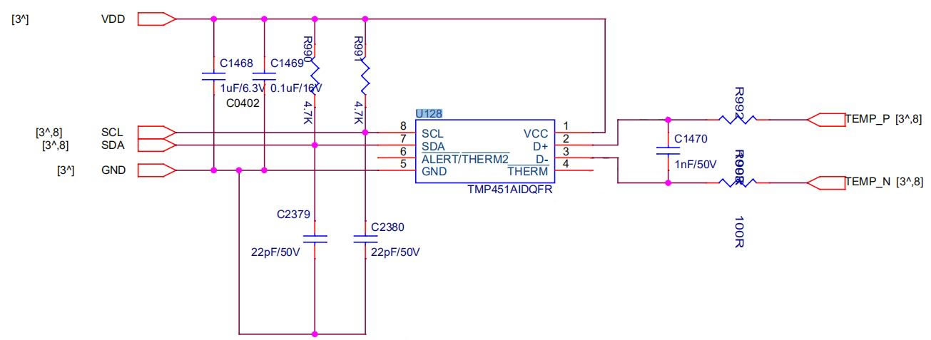
Figure 5-13
Figure 5-14
Check the quality of the front and back chip heat sinks connected to the temperature sensor. If the heat sink is not welded well, it will affect the temperature difference.
VI. Problems caused by control board issues
1. The whole machine is not running
First step: check whether the voltages at several voltage output points are normal. You can disconnect U8 first if 3.3V short circuit. If the short circuit still exists, you can unplug the CPU for measurement. For other voltage abnormalities, replace the corresponding transformer IC in general.
Second step: if the voltage is normal, please check the welding status of DDR / CPU (X-RAY inspection on the production side).
Third step: try to update the flash program with the SD card.
Figure 6-1
2.The whole machine cannot find the IP
Probably the IP is not found due to abnormal operation. Refer to point 1 for troubleshooting.
Check the appearance and soldering of the network port, network transformer T1, and CPU.
3. The whole machine cannot be upgraded
Check the appearance and soldering of the network port, network transformer T1, and CPU.
4.The whole machine fails to read the hashboard or has fewer chains
A. Check the cable connection
B. Check the parts of corresponding chain on the control board
C. Check the wave soldering quality of the pins and the resistance around the plug-in interface
VII. Machine failure
1. Initial test of the whole machine
With reference to the test process documents, the general problems are assembly process issues and control board process issues.
Common phenomena: IP is not detected, the number of fans is abnormal, and the chain is abnormal.
2. The whole machine sweeping frequency band
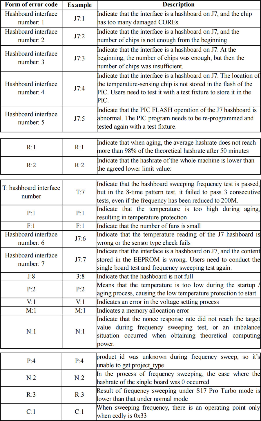
Refer to the definition of bad code for scanning during frequency sweeping, refer to Table 7-1
3. Machine aging and mining farm operation section
Low aging hashrate: Check the hashrate deviation of the corresponding hashboard, check if there is a large computing power difference. Take out the hashboard with a large hashrate difference for testing and maintenance. Check if the network has a low average hashrate caused by interruption.
Large aging temperature difference: check the aging environment; for high-temperature boards, check the soldering quality of the heat sinks of the hashboard.
Aging machine protection: Generally it is over temperature protection. Please control the aging environment temperature to be less than 40 degrees Celsius.

Figure 7-1
Less chain:
If one of the chains cannot be detected, the machine shall be disassembled and tested on the corresponding hashboard; if the hashboard is determined to be faulty, the hashboard shall be repaired, and if the control board is tested to be faulty, the control board shall be repaired.
4.After-sales maintenance
Refer to the above steps for troubleshooting. For related test procedures and use of test fixtures, please communicate with the after-sales engineer for details of the use. After repair, you can use the non-scanning mode to test PT2.
VIII. Other matters needing attention
Maintenance flowchart

Figure 8-1 Maintenance flowchart
• Routine test: first perform visual inspection on the hashboard to be repaired, observe whether the PCB is deformed or burnt. If yes, it must be handled first; check whether there are any parts with obvious burn marks, collision offset or missing parts, etc.; secondly, if no problem is found through visual inspection, the impedance of each voltage domain can be tested first to detect whether there is a short circuit or an open circuit. If yes, it must be handled first. Third, check whether the voltage of each domain is about 1.5V.
• After the routine test is OK (in general, the short-circuit test is necessary for the routine test to prevent the chip or other materials from being burned due to short circuit when the power is on), you can use the test fixture to perform chip detection, and determine the positioning based on the test fixture test results.
• According to the display result of the test fixture test, test the voltages of chip test points (CO / NRST / RO / XIN / BI), VDD0V8 and VDD1V8, etc. starting from the vicinity of the faulty chip.
• According to the signal direction (the RX signal is passed in the reverse direction (from chip 65 to 1), and several signals CLK CO BO RST are transmitted in the forward direction (from chip 1 to 65), find the abnormal fault point through the power supply sequence.
• When locating to the faulty chip, the chip needs to be re-soldered. The method is to add a flux around the chip (preferably no-clean flux), and heat the solder joints of the chip pins to a dissolved status, so as to promote the chip pins and the pads to re-run, then removing tin finally, thus achieving the effect of re-tinning. If the failure is the same after re-soldering, the chip shall be replaced directly.
• The repaired hashboard can be determined to be a good product if it passes the fixture tests for more than twice. For the first time, after the replacement of the accessories is complete, wait for the hashboard to cool down and perform fixture test, after passing, set it aside and then cool it down; for the second time, wait for a few minutes until the hashboard is completely cooled before testing.
• After the board is repaired, relevant maintenance / analysis records (requirements for maintenance reports: date, SN, PCB version, tag number, bad cause, bad liability attribution, etc.) should be prepared for feedback to production, after-sales, research and development departments.
• After the record is prepared, install the entire machine for conventional aging.
• Good products repaired at the production end should flow production from the first station of production (at least conduct the appearance inspection and start from the PT1 / PT2 test station)!
Your email address will not be published.Required fields are marked. *
Условия доставки
Доставляем по всей России
Транспортными компаниями от 2 дней
Условия возврата
-
Описание
-
Отзывы
-
Руководство по ремонту хэшплат Bitmain T17
от клиентов
отзывы о наших товарах

Новичок в майнинге
Вчера получил 4 посылку. Как всегда всё отлично. Ребята в Aslc-service.pro знают своё дело. Заказывал универсальный тестер для хеш плат чипы на с9 и процессор на контрольную плату. Весь товар как всегда отличного качества. От души благодарю всю команду Aslc-service.pro за отличный сервис и порядочность. И отдельная благодарность саппорту в телеге @AsicSupport за оперативную работу и помощь по любым вопросам касательно магазина Aslc-service.pro. Однозначно буду заказывать только у этих ребят. Доставка в Казахстан 6-7 дней сдэк.
Sabotage
Новичок в майнинге
В очередной раз от души благодарю всю команду asic-service.pro за отличный сервис и порядочность! Как всегда всё на высоте! Получил уже 3 заказа и со дня на день жду четвёртый! Ребята работают отлично! Качество товара всегда на высоте! Отправляют в день заказа если не выходные. Менеджер продаж всегда на связи в телеге! А вот менеджеру по продажам @AsicSupport отдельная благодарность! Всегда подскажет объяснит и поможет если что не понятно! Короче приятно иметь дело с такими людьми! И ещё в последнем заказе прислали не дешёвый такой бонус в виде 4х 5гр шприцев термопасты! Короче заказывать буду теперь только в asic-service.pro однозначно!
Доставка в Казахстан 6-7 дней Сдэк.
Михаил
Новичок в майнинге
От души благодарю всю команду Asic Service Pro за отличную работу и порядочность
Denis
Майнер со стажем
Всё чётко, заказывал в Иркутск себе сдеком, всё пришло что нужно
Благодарю
Арсений
Новичок в майнинге
Всё отлично. Заказывал разъемы и резисторы. Пришли сдэком за 3 дня. Хороших клиентов!
Дмитрий
Майнер со стажем
Сделка состоялась по «Вентилятор для L3+ и S9 6000 об./мин»
Все ок +1 , отправлял в Сибирь !
Пользователь
Майнер со стажем
Всё чётко, как и договаривались
Андрей

Майнер со стажем
Грамотно ответили и оперативно отправили
Денис
Новичок в майнинге
Все супер. Брал разные разъемы, ждал пока придут из Китая. После оплаты сразу отправили СДЭКом,как и просил. Все пришло,все как и заказывал.
Майнер со стажем
Заказывал хеш плату на асик s9, продавец в тот же день отправил, через 5 дней получил посылку, плата работает проблем нет.
Без опыта
Отправляют оперативно, заказывал разъёмы питания и косы БП. Общение радует. Всё отлично
Майнер со стажем
Часто беру у ребят комплектующие, качество хорошое, могут быстро привезти то чего здесь не достать. Спасибо
На этом сайте используются файлы cookie. Продолжая просмотр сайта, вы разрешаете их использование. Подробнее. Закрыть
В 23.11.2020 в 20:49, DeathOfPower сказал:
Кто-нибудь ремонтировал хэшплаты Antminer T17 или S17? Долго ли они работают после ремонта?
У меня вот такой опыт:
Antminer T17После почти что года работы на стандартной прошивке сдохла одна хэшплата. При инициализации определялись только 24 чипа из 30. Асик стоял на балконе в шумопоглощающем ящике, что продают на Авито. От ящика до балконного окна с антикомариной сеткой были проложены 2 алюминиевые гофры чтобы горячий воздух выдувался за борт. Зимой при морозах асик тоже отлично работал. Остекление балкона хоть и есть но обычным одинарным стеклом, не стеклопакетами.
Сразу чинить не понёс — то некогда то отпуск. Потом сдохла вторая плата — в логе было что-то про питание, мол 0 вольт на плате. В итоге отнёс сразу 2 платы в ремонт. Забрал через неделю. Поставил — одна плата работает, на второй определяются 0 чипов. Тогда на улице было +5-7 градусов. Отнёс незаработавшую плату по гарантии (1 месяц). Пока её ремонтировали на той плате что сразу заработала через 2 дня 6 чипов перестали давать хэшрейт (после ремонта установил прошивку от Vnish — она позволяет задавать какую температуру чипов поддерживать ну и понижать напряжение чтоб меньше жрало электричества). При инициализации определяются все 30 а когда начинается майнинг у шести чипов хэшрейт — 0. Даже при стандартном напряжении и частоте.
Когда забирал одну плату из повторного ремонта отдал сразу вторую в повторный ремонт. В этот раз незаработавшая плата завелась и нормально работала. За это время сдохла 3-я плата — видит 24 чипа из 30.
Потом поехал забрал вторую плату из повторного ремонта. Привёз домой воткнул — не работает. При инициализации определяются то 17, то 24 то 6 то 1 чип. Отвёз её обратно. На следующий день звонят — мы подключили у нас работает. Повёз сам асик. У них подключили, вставили плату — работает. Привёз домой — в комнате включил — работает. Отнёс в ящик на балкон. Включаю — опять определяются то 17, то 24 то 6 то 1 чип.
Позвонил в сервис — говорят мол 17-я серия капризная им надо чтобы не меньше 15 градусов было в помещении. Но как это может быть? В инструкции пишут что рабочая температура окружающей среды от 0 до +25. Почему после ремонта надо вдруг не ниже 15 градусов?
В общем помайнил одной картой пару дней чтобы добраться до порога вывода намайненного с пула. Занёс опять домой. Постоял он часа 2, нагрелся. Включаю — та плата уже и в тепле не работает — определяются 24 чипа из 30. И что самое противное та плата что проработала дней 10 после ремонта тоже перестала запускаться — пишет 0 чипов из 30 найдено.
Вот и думаю — стоит ли пробовать ремонтировать 3-ю плату в другом месте, или лучше продать на запчасти. Блок питания то и управляющая плата в порядке. А с хэшплат можно повыпаивать чипы и отобрать нормальные.
у 17 серии есть проблемка в припое, он хрупкий. похоже на то, что микротрещины в пайке образовались. обычно лечится прогревом плат до 200 градусов, в течении пары минут